Why yet another overview blog on High-Level Synthesis (HLS), you may ask – and I was wondering all the same. But with the latest releases of AMD’s Vitis Unified IDE and the Vitis HLS libraries available, it may be interesting to revisit the adoption of HLS for the community.
In this and subsequent articles, we will highlight hotspots of working with HLS component design.

Principal HLS project
The core proposition of the high-level synthesis toolchain from AMD is to convert a C/C++ code base into a synthesizable netlist, that can further be used in designs for the lineup of AMD adaptive SoCs, FPGAs, and SOMs. With this approach, the design efficiency will be improved by achieving proper function closure on the C/C++-level and only then diving into hardware synthesis and implementation. This allows commonly a high design iteration throughput.
Along such projects, various interesting aspects are typically encountered and we will cover such one at a time, while this first issue of this mini-series will derive an overview of the project flow to set the scope for the upcoming issues. Of course, we will also timely catch up with any inputs that you may raise with questions of your own journey.
Baselining
HLS component generation starts with a C-based design and converts it into verified Register Transfer Level (RTL) through the HLS compiler. This compiler has to analyze the C-code to:
- create the respective function’s operations.
- assign the resources for the data registers.
- anything in between, which can be additional buffers, shift registers, state machine logic, and other basic design elements.
In order to create these design elements correctly the project must hold the device technology information, simply by selecting a target device and an overall performance bound, which is the clock rate to be achieved. This will be used to guide the compiler to reach for higher performance by reducing the logic cycles used per function and further replicating any congested logic as would limit the original performance of a standard processor. This typically yields a clear FPGA advantage for offloading dense computation from the CPU cores.
Over releases the Vitis HLS Compiler grew to high quality to yield a verified synthesizable RTL netlist. A reasonable C/C++ Code guided by obvious principles will be synthesized by the compiler out of the box, which is commonly referred to as baseline.
Project Walkthrough
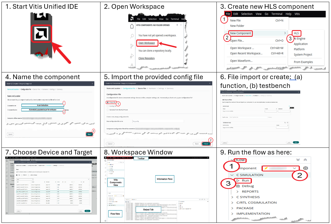
Follow the flow in Img 2 to generate a full project and yield a generated IP from a C/C++ code base.
The resulting Vitis HLS component already exhibits a distinct performance that is presented with different focus in multiple analyzers in the GUIs. Such reports include the Synthesis Summary Report, Schedule Viewer, Function Call Graph, and Dataflow Viewer. This will give rise to actions towards optimization later on. You may want to familiarize yourself with the respective outputs.
Project Walkthrough
Summary
This blog entry sets the scope for iterations on HLS issues. So far the resulting synthesizable RTL code has not been adapted for any concrete performance requirements, nor have we considered any C/C++ code changes or added directives to achieve a particular implementation. This is considered a baseline and all improvements will start from here.
Along with the FPGA benefits predicted earlier, the compiler may have achieved a suitably fast base cycle as given by the project target and also »perfect« parallelism. The metric to asses this is the initiation interval (II), telling basically how often a certain path can be fed for contributing to the output.
An II = 1 implies that the resulting design digests a new data item per each clock cycle, which is obviously the best case in sequential circuits.
In the next instalment of the HLS mini-series, we will be handling variable loop depths. If you would like to deep dive in the world of HLS right now, sign up for PLC2’s training course Compact Vitis HLS and benefit from 2 hours of free coaching support with every training session you book.