FPGA Design Techniques
Clock Domain Crossing (CDC)
In the last blog post, we talked about timing exceptions and how they can be implemented. However, defining timing exceptions is not enough to achieve a reliable CDC design.
Let us assume that the following circuit is implemented:
ClkA and ClkB have different clock frequencies, are not related, and the phase of the clocks is unknown.
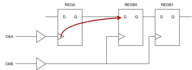
Figure 1: CDC circuit
There are existing time points, at which the flip-flop REGB0 will become metastable, because at some point, the setup or hold time requirement will be violated. This means that REGB0 is not switching correctly from 0 to 1 or from 1 to 0, depending on the input data connected to port D of REGB0. Instead of switching immediately, the data output Q may oscillate, which means, that the value of Q is somehow floating between the value 0 and 1. Depending on the technology, clock frequencies, and environmental conditions, the value of Q eventually resolves to a static 0 or 1 after some time.
This behaviour results in situations where your digital circuit is not behaving as intended. The following example will describe a situation where this is the case:
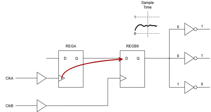
Figure 2: Extended CDC circuit
The example is extended by three inverters that are connected to the output Q of REGB0. As shown in the image above, REGB0 is getting metastable while switching from 0 to 1. As explained earlier, the value is somehow changing between 0 and 1. Because of routing length differences and other factors, it may happen, that the three inverters are not sampling the same value at the same time. In this example, two inverters are sampling a 0 while one inverter is sampling a 1. This results in an output of »110« when reading the inverter outputs from top to bottom. This value is not expected and can lead to unpredictable behaviours in other parts of the circuit which is connected to the outputs of the inverters.
Various methods for adressing and solving this and related situations will be discussed in the following blogs posts, focusing on digital design techniques in FPGAs.
If you would like to deepen your expertise on timing constraints and digital circuit designs, join our »Compact Timing Constraints and Analysis« or »Compact Circuit Design Techniques« training, and take your skills to the next level.