In many cases, it is the designer’s choice to implement an asynchronous or a synchronous circuit design in an FPGA. In the last article, the differences between the two types of circuits were discussed. In this article, our focus is to discuss one of the most important rules and most needed methodologies for synchronous design techniques.
Every design needs to have an additional slow clock, compared to the master clock, with which most of the FPGA design is running. In the following example, a clock with half of the frequency of the existing clock is needed.
The intuitive way (but not the best way) to achieve this is shown below:
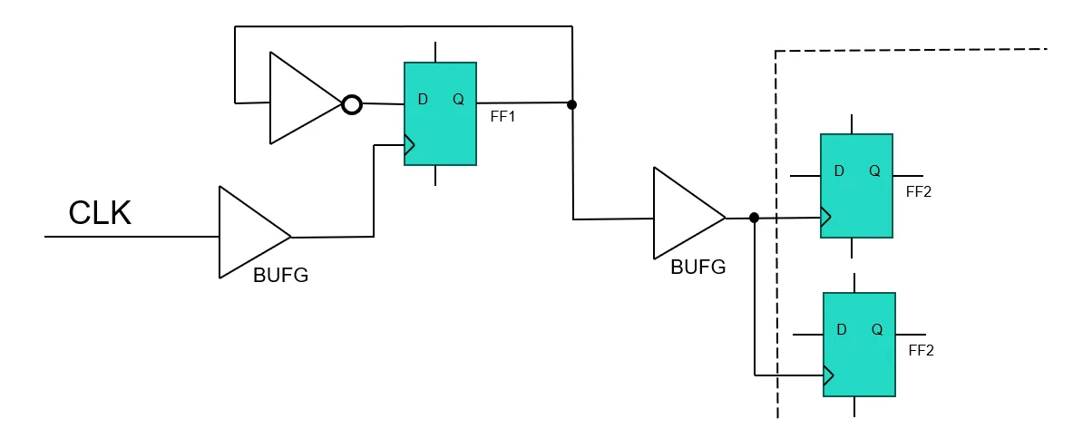
Figure 1: Clock divider
The circuit consists of a toggle flip-flop FF1, which is followed by an additional BUFG, providing a clock of half the frequency of CLK to another clock domain, to which the two flip-flops FF2 and FF3 belong to. In general, this circuit is working if CLK and clock which is generated by FF1, do not have any points of contact. It is important to know that the two clocks are not in phase and that they should be treated as asynchronous clocks rather than synchronous clocks that are in phase, which is a disadvantage of the design above. An additional disadvantage is that we are using two BUFGs.
There is a better way to implement the functionality by creating a synchronous circuit. As shown below:
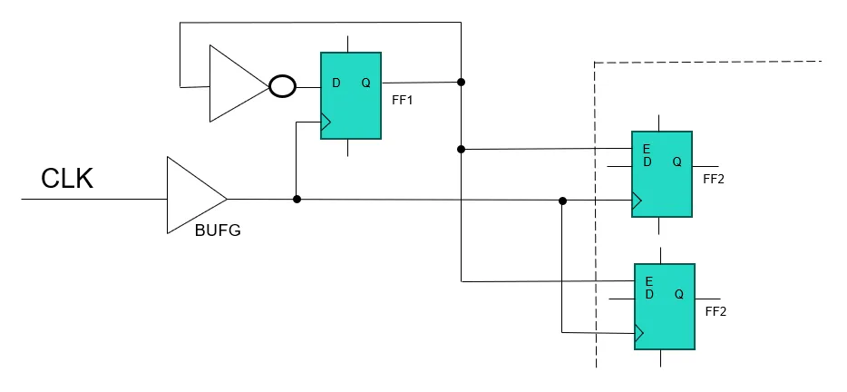
Synchronous circuit
The idea of the synchronous clock divider shown above is like the clock divider which was shown as a first example. We still need a toggle flip-flop to generate a signal which is toggling with half the frequency of CLK. The advantage of this circuit is, that data output of FF1 is not used as a clock. As seen in the block diagram above, the data output is used to control the enable inputs (CE) of FF2 and FF3. By designing the circuit in this way, a second BUFG is not needed. The circuit can also be considered as synchronous. All flip-flops are connected to the same clock (CLK). This is another big advantage because we do not have to care about CDCs.
By comparing the two circuits, we can observe that both circuits are behaving the same, while the second circuit does not have the disadvantages of the first circuit.
In the following blog posts, we will discuss more related situations, focusing on digital design techniques in FPGAs.
If you would like to go deeper into other digital design topics and principles, they are covered in detail in our 5-day »Professional FPGA Circuit Design Technique« training.