When it comes to clocked digital design circuits, there are two ways to implement a digital circuit. One option is to use an asynchronous approach. This means that not all of the involved clocked elements are synchronised with the same clock.
Let us look at an example:
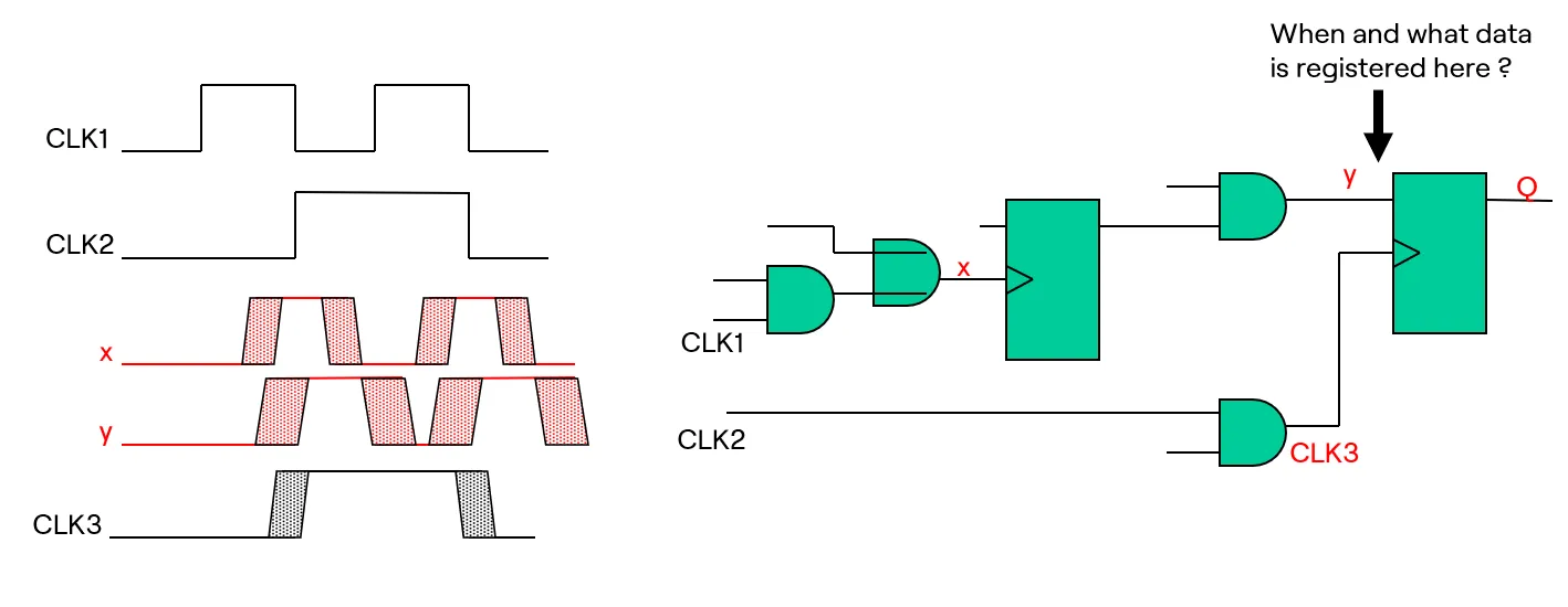
Figure 1: Asynchronous circuit
As you can see in figure 1, CLK1 is going through two and gates before arriving at the first flip-flop. The timing diagram on the left shows that there is a possible arrival time interval. This is because the propagation delay through combinatorial logic depends on voltage, temperature, and process. Looking at the temperature reveals that the clock x is arriving faster at the flip-flop when the temperature is low, and it slower when the temperature is high. The same is happening for the signal y, also due to the and gate in the data path between the two flip-flops. Additionally, CLK2 is also going through an and gate resulting in CLK3 and arriving at the second flip-flop. As a result, we can see that there are different arriving times for the signals x, y and CLK3 possible.
Even in this simple example, we have to make a significant effort to verify that the above circuit works in every possible condition, taking into account environmental factors such as voltage, temperature and process. If we consider that this circuit is implemented in an FPGA, it is possible that the routing length and the elements used are different when the FPGA design is updated or extended, because it will have to be reimplemented.
This means that the circuit must be verified again, even if it has been verified before, due to different routing lengths, for example. This can be very time-consuming.
When using an FPGA, it is likely that we will want to make changes over time and reimplement the FPGA design after updating the VHDL code. In this case, designing a synchronous circuit is much more reliable and simpler. In a synchronous circuit, all the clocked elements are connected to the same clock. Additionally, we should avoid connecting any combinatorial logic to the clock network to prevent introducing delays into the clock.
Let us look at the following example, which shows a synchronous circuit:
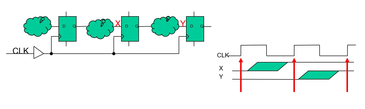
Synchronous circuit
As previously explained, there is no combinatorial logic connected to the clock, and all clocked elements are connected to the same clock. As can be seen, there is only combinatorial logic in the data path (shown as clouds). As can be seen on the right, signals X and Y arrive at the specific flip-flops sooner or later. This is due to environmental factors such as temperature, voltage and process.
The major advantage of synchronous circuits is variations in data line delay, dependent on environmental factors, always occur between clock (CLK) rising edges. This circuit always runs at the same speed (clock frequency), regardless of whether the data arrives sooner or later at the flip-flop. It is sufficient to verify this circuit once. As long as the setup and hold times of the flip-flops are not violated, the circuit always works independently of routing lengths or delays. This is why synchronous designs are generally preferable to asynchronous designs. However, there are special cases where it can be necessary to implement asynchronous designs as well.
If you would like to go deeper into other digital design topics and principles, they are covered in detail in our 5-day »Professional FPGA Circuit Design Technique« training.