The AMD Zynq UltraScale+ RFSoC enables a highly integrated RF system architecture by combining high-speed ADCs and DACs with FPGA fabric on a single device. This integration is particularly valuable in wideband electronic analysis systems, where large portions of the RF spectrum must be monitored and reacted to with minimal latency. A block diagram is shown below:
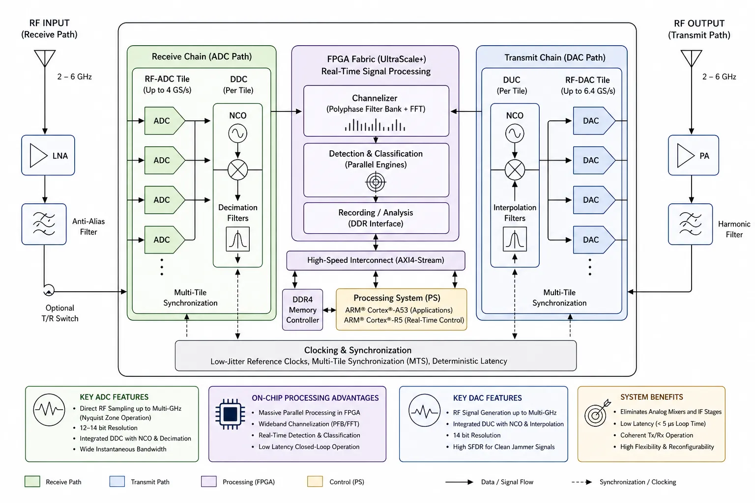
RFSoC system overview
In conventional RF systems, incoming signals are downconverted using analog mixers before digitization, and transmitted signals require corresponding upconversion stages after the DAC. These analog components introduce nonlinearity, phase noise, calibration effort, and additional latency. The RFSoC removes these stages by enabling direct RF sampling.
In a typical receiver chain, the antenna signal is first conditioned by a minimal analog frontend consisting of amplification and filtering. It is then directly digitized by the integrated RF-ADC operating at multi-gigasample-per-second rates. This allows signals in the gigahertz range to be captured without intermediate frequency stages. The ADC tiles include built-in digital downconversion, where numerically controlled oscillators and decimation filters translate the signal into baseband and reduce the data rate.
The resulting data is processed inside the FPGA fabric, where wideband channelization is typically implemented using polyphase filter banks and FFT-based techniques. This enables parallel monitoring of many narrowband channels across a wide spectrum. Detection, classification, and recording can all be performed in real time due to the high degree of parallelism.
On the transmit side, responses are generated digitally in the FPGA. These baseband signals are passed to the RF-DAC, which includes integrated digital upconversion and interpolation filtering. The DAC then generates the RF signal directly, eliminating the need for analog upconversion. The output can be fed directly into a power amplifier and antenna, simplifying the RF frontend and improving signal quality.
A key advantage of this architecture is the closed-loop operation entirely within the chip. Signals can be received, processed, and retransmitted within microseconds, enabling rapid reaction. Because ADC and DAC share the same clocking infrastructure, the system can operate coherently, which is essential for some use cases.
The integrated approach also provides deterministic latency, high bandwidth, and excellent reconfigurability. Frequency tuning, bandwidth adaptation, and waveform changes can all be implemented in software or FPGA logic without hardware modifications.
However, the design also introduces challenges, including extremely high internal data rates, increased thermal density, and strict requirements on clock quality. Careful system design is required to fully exploit the capabilities of the device.
Overall, the integration of high-speed ADCs and DACs in the AMD Zynq UltraScale+ RFSoC fundamentally changes RF system design. It enables compact, flexible, and low-latency architectures that are well suited for demanding applications such as, radar, and next-generation communication systems.
If you would like to go deeper into other digital design topics and principles, they are covered in detail in our 5-day »Professional FPGA Circuit Design Technique« training.